标签:模拟电子技术基础,模拟电子电路,http://www.5idzw.com
ADC中的ABC:理解ADC误差对系统性能的影响,The A,http://www.5idzw.com
With systems that do a one-time temperature calibration, it's important to pay heed to the drift specs. If the initial offset is calibrated and the temperature moves, there will be an error introduced due to the drift term that can negate the effects of the calibration. For example, assume a reading is done at temperature X. Some time later, the temperature has changed 10°C and the exact same measurement is taken. These two readings can give different results, calling into question the repeatability and thus the reliability of the system.
There is a good reason why manufacturers do not give maximum limits: This increases the cost. Drift testing requires special boards, and an extra step must be added to the test flow (which equates to an additional manufacturing cost) to make sure the parts do not exceed the maximum-drift limit.
Gain drift is more of an issue, particularly for devices tested with an internal reference. In this case, the reference drift can be included in the gain-drift parameter. For an external reference, the IC's gain drift is typically fairly small, like 0.8ppm/°C. Thus, a +/-10 degree temperature change results in a +/-8ppm change. Note that 12-bit performance equates to 244ppm (1/4096 = 0.0244% = 244ppm). So, we see an error that represents only a fraction of an LSB at the 12-bit level.
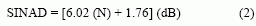
where N is the number of bits. For an ideal 12-bit converter, the SINAD is 74dB. Should this equation be rewritten in terms of N, it would reveal how many bits of information are obtained as a function of the RMS noise:
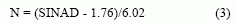
This equation is the definition for effective number of bits, or ENOB.
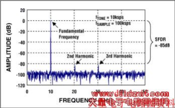
Figure 9. FFT plot reveals AC performance of an ADC.
Note that SINAD is a function of the input frequency. As frequency increases toward the Nyquist limit, SINAD decreases. If the specification in the data sheet is tested at low frequencies compared to the Nyquist frequency, you can bet the performance will be much worse near Nyquist. Look for an ENOB graph in the Typical Operating Characteristics of the data sheet. ENOB degrades with frequency primarily because THD gets increasingly worse as the input frequency increases. For example, with a SINAD minimum value of 68dB at the frequency of interest, you obtain an ENOB value of 11. Therefore, you have lost 1 bit of information due to the converter's noise and distortion performance. This means that your 12-bit converter can provide only 0.05% accuracy at best. Remember that INL is a DC spec; ENOB is the specification that tells about nonlinearities for AC signals.
SNR is the signal-to-noise ratio with the distortion components removed. SNR reveals where the noise floor of the converter is. There can be a steep decrease in SNR as a function of input frequency, which means the converter was not designed for frequencies near this point. One way to improve SNR is to oversample, which provides a processing gain. Oversampling is a method of lowering the noise floor of the converter by sampling at a rate much higher than the signal of interest. This spreads the noise out over a wider range in the frequency domain, thereby effectively reducing the noise at any one frequency bin. A 2X oversampling reduces the noise floor by 3dB.
,ADC中的ABC:理解ADC误差对系统性能的影响,The A
Load Regulation
The final spec is reference load regulation. Often the voltage reference used for an ADC has ample current to drive other devices, so it is used by other ICs. The current drawn by those other components will affect the voltage reference, which means that as more current is drawn the reference voltage will droop. If the devices using the reference are turning on and off intermittently, the result will be a reference voltage that moves up and down. A 0.55µV/µA reference-load-regulation specification for a 2.5V reference means that, if other devices draw 800µA, the reference voltage will change up to 440µV, which is .0176% (440µV/2.5V) or almost 20% of the available error margin.Other Temperature Effects
Continuing with the topic of temperature, two specifications that are often given little attention are offset drift and gain drift. These specs are usually given as typical numbers only, leaving it up to the users to determine if the specification is good enough for their system requirements. Offset- and gain-drift values can be compensated in a couple of different ways. One way is to fully characterize the offset and gain drift, and provide a lookup table in memory to adjust the values as temperature changes. This, however, is a cumbersome process, as each ADC must be compensated individually and the compensation process is a time-consuming effort. The second method is to perform calibrations when a significant temperature change has occurred.With systems that do a one-time temperature calibration, it's important to pay heed to the drift specs. If the initial offset is calibrated and the temperature moves, there will be an error introduced due to the drift term that can negate the effects of the calibration. For example, assume a reading is done at temperature X. Some time later, the temperature has changed 10°C and the exact same measurement is taken. These two readings can give different results, calling into question the repeatability and thus the reliability of the system.
There is a good reason why manufacturers do not give maximum limits: This increases the cost. Drift testing requires special boards, and an extra step must be added to the test flow (which equates to an additional manufacturing cost) to make sure the parts do not exceed the maximum-drift limit.
Gain drift is more of an issue, particularly for devices tested with an internal reference. In this case, the reference drift can be included in the gain-drift parameter. For an external reference, the IC's gain drift is typically fairly small, like 0.8ppm/°C. Thus, a +/-10 degree temperature change results in a +/-8ppm change. Note that 12-bit performance equates to 244ppm (1/4096 = 0.0244% = 244ppm). So, we see an error that represents only a fraction of an LSB at the 12-bit level.
AC Performance
Some ADCs perform well only with input signals at or near DC. Others perform well with input signals from DC up to Nyquist. Just because DNL and INL meet the system requirements does not mean the converter will give that same performance when AC signals are considered. DNL and INL are DC tests. We must look to the AC specs to get a good feeling for AC performance. The Electrical Characteristics table and the Typical Operating Characteristics found in the data sheet offer clues to the AC performance. The key specs to review are signal-to-noise ratio (SNR), signal-to-noise and distortion ratio (SINAD), total harmonic distortion (THD), and spurious-free dynamic range (SFDR). The first specification to review is SINAD or SNR. SINAD is defined as the RMS value of an input sine wave to the RMS value of the noise of the converter (from DC to the Nyquist frequency, including harmonic [total harmonic distortion] content). Harmonics occur at multiples of the input frequency (see Figure 9). SNR is similar to SINAD, except that it does not include the harmonic content. Thus, the SNR should always be better than the SINAD. Both SINAD and SNR are typically expressed in dB.where N is the number of bits. For an ideal 12-bit converter, the SINAD is 74dB. Should this equation be rewritten in terms of N, it would reveal how many bits of information are obtained as a function of the RMS noise:
This equation is the definition for effective number of bits, or ENOB.
Figure 9. FFT plot reveals AC performance of an ADC.
Note that SINAD is a function of the input frequency. As frequency increases toward the Nyquist limit, SINAD decreases. If the specification in the data sheet is tested at low frequencies compared to the Nyquist frequency, you can bet the performance will be much worse near Nyquist. Look for an ENOB graph in the Typical Operating Characteristics of the data sheet. ENOB degrades with frequency primarily because THD gets increasingly worse as the input frequency increases. For example, with a SINAD minimum value of 68dB at the frequency of interest, you obtain an ENOB value of 11. Therefore, you have lost 1 bit of information due to the converter's noise and distortion performance. This means that your 12-bit converter can provide only 0.05% accuracy at best. Remember that INL is a DC spec; ENOB is the specification that tells about nonlinearities for AC signals.
SNR is the signal-to-noise ratio with the distortion components removed. SNR reveals where the noise floor of the converter is. There can be a steep decrease in SNR as a function of input frequency, which means the converter was not designed for frequencies near this point. One way to improve SNR is to oversample, which provides a processing gain. Oversampling is a method of lowering the noise floor of the converter by sampling at a rate much higher than the signal of interest. This spreads the noise out over a wider range in the frequency domain, thereby effectively reducing the noise at any one frequency bin. A 2X oversampling reduces the noise floor by 3dB.
,ADC中的ABC:理解ADC误差对系统性能的影响,The A
上一篇:ad9850电路