标签:模拟电子技术基础,模拟电子电路,http://www.5idzw.com
ADC中的ABC:理解ADC误差对系统性能的影响,The A,http://www.5idzw.com
Figure 1a. DNL error: no missing codes.
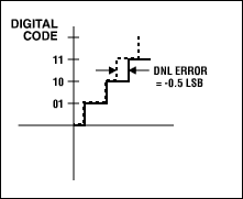
Figure 1b. DNL error: no missing codes.
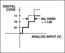
Figure 1c. DNL error: Code 10 is missing.
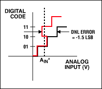
Figure 1d. DNL error: At AIN* the digital code can be one of three possible values. When the input voltage is swept, Code 10 will be missing.
When DNL-error values are offset (that is, -1LSB, +2LSB), the ADC transfer function is altered. Offset DNL values can still in theory have no missing codes. The key is having -1LSB as the low limit. Note that DNL is measured in one direction, usually going up the transfer function. The input-voltage level required to create the transition at code [N] is compared to that at code [N+1]. If the difference is 1LSB apart, the DNL error is zero. If it is greater than 1LSB, the DNL error is positive; if it is less than 1LSB, the DNL error is negative.
Having missing codes is not necessarily bad. If you need only 13 bits of resolution and you have a choice between a 16-bit ADC with a DNL specification < = +/-4LSB DNL (which is effectively 14 bits, no missing codes) that costs $5 and a 16-bit ADC with a DNL of < = +/-1LSB that costs $15, then buying the lower-grade version of the ADC will allow you to greatly reduce component cost and still meet your system requirements.
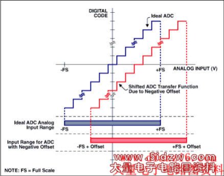
Figure 2. Bipolar offset error.
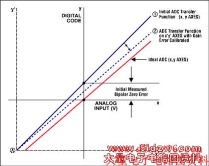
Figure 3a.
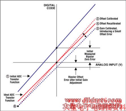
Figure 3b.
Figures 3a and 3b. Calibrating bipolar offset error. (Note: The stair-step transfer function has been replaced by a straight line, because this graph shows all codes and the step size is so small that the line appears to be linear.)
Unipolar systems are a little trickier. If the offset is positive, use the same methodology as that for bipolar supplies. The difference here is that you lose part of the ADC's range (see Figure 4). If the offset is negative, you cannot simply do a conversion and expect the result to represent the offset error. Below zero, the converter will just display zeros. Thus, with a negative offset error, you must increase the input voltage slowly to determine where the first ADC transition occurs. Here again you lose part of the ADC range.
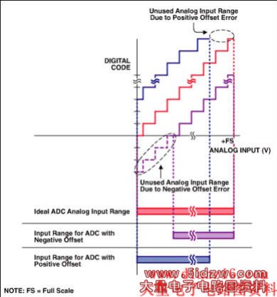
Figure 4. Unipolar offset error.
Returning to our example, two scenarios for offset error are given below:
Figure 1a. DNL error: no missing codes.
Figure 1b. DNL error: no missing codes.
Figure 1c. DNL error: Code 10 is missing.
Figure 1d. DNL error: At AIN* the digital code can be one of three possible values. When the input voltage is swept, Code 10 will be missing.
When DNL-error values are offset (that is, -1LSB, +2LSB), the ADC transfer function is altered. Offset DNL values can still in theory have no missing codes. The key is having -1LSB as the low limit. Note that DNL is measured in one direction, usually going up the transfer function. The input-voltage level required to create the transition at code [N] is compared to that at code [N+1]. If the difference is 1LSB apart, the DNL error is zero. If it is greater than 1LSB, the DNL error is positive; if it is less than 1LSB, the DNL error is negative.
Having missing codes is not necessarily bad. If you need only 13 bits of resolution and you have a choice between a 16-bit ADC with a DNL specification < = +/-4LSB DNL (which is effectively 14 bits, no missing codes) that costs $5 and a 16-bit ADC with a DNL of < = +/-1LSB that costs $15, then buying the lower-grade version of the ADC will allow you to greatly reduce component cost and still meet your system requirements.
INL
INL is defined as the integral of the DNL errors, so good INL guarantees good DNL. The INL error tells how far away from the ideal transfer-function value the measured converter result is. Continuing with our example, an INL error of +/-2LSB in a 12-bit system means the maximum nonlinearity error may be off by 2/4096 or 0.05% (which is already about two-thirds of the allotted ADC error budget). Thus, a 1LSB (or better) part is required. With a +/-1LSB INL error, the accuracy is 0.0244%, which accounts for 32.5% of the allotted ADC error budget. With a specification of 0.5LSB, the accuracy is 0.012%, and this accounts for only about 16% (0.012%/0.075%) of our ADC error budget limit. Note that neither INL nor DNL errors can be calibrated or corrected easily.Offset and Gain Errors
Offset and gain errors can easily be calibrated out using a microcontroller (µC) or a digital signal processor (DSP). With offset error, the measurement is simple when the converter allows bipolar input signals. In bipolar systems, offset error shifts the transfer function but does not reduce the number of available codes (Figure 2). There are two methodologies to zero out bipolar errors. In one, you shift the x and y axes of the transfer function so that the negative full-scale point aligns with the zero point of a unipolar system (Figure 3a). With this technique, you simply remove the offset error and then adjust for gain error by rotating the transfer function about the "new" zero point. The second technique entails using an iterative approach. First apply zero volts to the ADC input and perform a conversion; the conversion result represents the bipolar zero offset error. Then perform a gain adjustment by rotating the curve about the negative full-scale point (Figure 3b). Note that the transfer function has pivoted around point A, which moves the zero point away from the desired transfer function. Thus, a subsequent offset-error calibration may be required. Figure 2. Bipolar offset error.
Figure 3a.
Figure 3b.
Figures 3a and 3b. Calibrating bipolar offset error. (Note: The stair-step transfer function has been replaced by a straight line, because this graph shows all codes and the step size is so small that the line appears to be linear.)
Unipolar systems are a little trickier. If the offset is positive, use the same methodology as that for bipolar supplies. The difference here is that you lose part of the ADC's range (see Figure 4). If the offset is negative, you cannot simply do a conversion and expect the result to represent the offset error. Below zero, the converter will just display zeros. Thus, with a negative offset error, you must increase the input voltage slowly to determine where the first ADC transition occurs. Here again you lose part of the ADC range.
Figure 4. Unipolar offset error.
Returning to our example, two scenarios for offset error are given below:
- If the offset error is +8mV, with a 2.5V reference this corresponds to 13LSBs of error for a 12-bit ADC (8mV/[2.5V/4096)]. Though the resolution is still 12 bits, you must subtract 13 codes from each conversion result to compensate for the offset error. Note that the actual, measurable, full-scale value in this scenario is now 2.5V (4083/4096) = 2.492V. Any value above this will over-range the ADC. So, the dynamic range, or range of input values, for the ADC has been reduced. This is even more important for higher-resolution ADCs; 8mV represents 210LSBs at the 16-bit level (VREF = 2.5V).
- If the offset is -8mV (assuming a unipolar input), then small analog-input values near zero will not register when a conversion is performed until the analog input exceeds +8mV. This too reduces the dynamic range of the ADC.
上一篇:ad9850电路