标签:模拟电子技术基础,模拟电子电路,http://www.5idzw.com
ADC中的ABC:理解ADC误差对系统性能的影响,The A,http://www.5idzw.com
Gain error is defined as the full-scale error minus the offset error (Figure 5). Full-scale error is measured at the last ADC transition on the transfer-function curve and compared against the ideal ADC transfer function. Gain error is easily corrected in software with a linear function y = (m1/m2)(x), where m1 is the slope of the ideal transfer function and m2 is the slope of the measured transfer function (Figure 5).

Figure 5. Offset, gain, and full-scale errors.
The gain-error specification may or may not include errors contributed by the ADC's voltage reference. In the electrical specifications, it is important to check the conditions to see how gain error is tested and to determine whether it is performed with an internal or external reference. Typically, the gain error is much worse when an on-chip reference is used. If the gain error were zero, when a conversion is performed the conversion result would begin to yield all ones (3FFh in our 12-bit example) when the full-scale analog input is applied (see Figure 6). As our converter is not ideal, you can initially end up with all ones in the conversion result when a voltage greater than full-scale is applied (negative gain error) or when a voltage less than full-scale is applied (positive gain error). Two ways to adjust for gain error are to either tweak the reference voltage such that at a specific reference-voltage value the output gives full-scale or use a linear correction curve in software to change the slope of the ADC transfer-function curve (a first-order linear equation or a lookup table can be used).
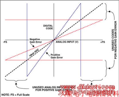
Figure 6. Gain error reduces dynamic range.
As with offset error, you lose dynamic range with gain error. For example, if a full-scale input voltage is applied and the code obtained is 4050 instead of the ideal 4096 (for a 12-bit converter), this is defined as negative gain error, and in this case the upper 46 codes will not be used. Similarly, if the full-scale code of 4096 appears with an input voltage less than full-scale, the ADC's dynamic range is again reduced (see Figure 6). Note that, with positive full-scale errors, you cannot calibrate beyond the point where the converter gives all ones in the conversion result.
The easiest way to handle offset and gain errors is to find an ADC with values low enough so that you don't have to calibrate. It's fairly easy to find 12-bit ADCs with offset and gain errors less than 4LSB.
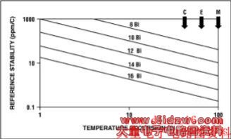
Figure 7. Voltage-reference-drift requirements relate to ADC resolution.
For some systems, the reference accuracy is not a big issue, as the temperature is held constant, eliminating the drift problem. Some systems use a ratiometric measurement, where the reference errors are removed because the same signal that excites the sensor is used as the reference voltage (Figure 8). Because the excitation source and reference move as one, drift errors are eliminated.
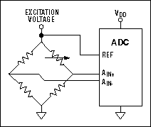
Figure 8. Ratiometric ADC conversion.
In other systems, calibration is performed often enough so that reference drift is effectively removed. In still other systems, absolute accuracy is not critical, but relative accuracy is. Therefore, the reference can drift slowly with time and the system will provide the desired accuracy.
,ADC中的ABC:理解ADC误差对系统性能的影响,The A
Gain error is defined as the full-scale error minus the offset error (Figure 5). Full-scale error is measured at the last ADC transition on the transfer-function curve and compared against the ideal ADC transfer function. Gain error is easily corrected in software with a linear function y = (m1/m2)(x), where m1 is the slope of the ideal transfer function and m2 is the slope of the measured transfer function (Figure 5).
Figure 5. Offset, gain, and full-scale errors.
The gain-error specification may or may not include errors contributed by the ADC's voltage reference. In the electrical specifications, it is important to check the conditions to see how gain error is tested and to determine whether it is performed with an internal or external reference. Typically, the gain error is much worse when an on-chip reference is used. If the gain error were zero, when a conversion is performed the conversion result would begin to yield all ones (3FFh in our 12-bit example) when the full-scale analog input is applied (see Figure 6). As our converter is not ideal, you can initially end up with all ones in the conversion result when a voltage greater than full-scale is applied (negative gain error) or when a voltage less than full-scale is applied (positive gain error). Two ways to adjust for gain error are to either tweak the reference voltage such that at a specific reference-voltage value the output gives full-scale or use a linear correction curve in software to change the slope of the ADC transfer-function curve (a first-order linear equation or a lookup table can be used).
Figure 6. Gain error reduces dynamic range.
As with offset error, you lose dynamic range with gain error. For example, if a full-scale input voltage is applied and the code obtained is 4050 instead of the ideal 4096 (for a 12-bit converter), this is defined as negative gain error, and in this case the upper 46 codes will not be used. Similarly, if the full-scale code of 4096 appears with an input voltage less than full-scale, the ADC's dynamic range is again reduced (see Figure 6). Note that, with positive full-scale errors, you cannot calibrate beyond the point where the converter gives all ones in the conversion result.
The easiest way to handle offset and gain errors is to find an ADC with values low enough so that you don't have to calibrate. It's fairly easy to find 12-bit ADCs with offset and gain errors less than 4LSB.
Other Subtle Error Sources
Code-Edge Noise
Code-edge noise is the amount of noise that appears right at a code transition on the transfer function. It is often not specified in the data sheet. Even higher-resolution converters (16+ bits), where code-edge noise is much more prevalent due to the smaller LSB size, will often not specify code-edge noise. Sometimes, code-edge noise can be several LSBs. Conversions performed with the analog input right at the code edge can result in code flicker in the LSBs. Significant code-edge noise means that an average of samples must be taken to effectively remove this noise from the converter results. How many samples are needed? If the code-edge noise is 2/3LSB RMS, this equates to approximately 4LSB p-p. Sixteen samples will have to be taken to reduce the noise to 1LSB (the square root of the number of samples determines the improvement in performance).The Reference
One of the biggest potential sources of errors in an ADC with an internal or external reference is the reference voltage. Often, if the reference is included on-chip, it is not specified adequately. To understand the source of the reference errors, it is important to look at three specs in particular: temperature drift, voltage noise, and load regulation.Temperature Drift
Temperature drift is the most overlooked specification in the data sheet. As an example, note how temperature drift affects the performance of an ADC converter based on resolution (Figure 7). For a 12-bit converter to maintain accuracy over the extended temperature range (-40°C to +85°C), the drift must be a maximum of 4ppm/°C. Unfortunately, no ADC converter is available with this kind of on-chip-reference performance. If we relax the requirements, a 10-degree temperature excursion means the 12-bit ADC reference can drift no more than 25ppm/°C, which again is a fairly tight requirement for on-chip references. Prototyping frequently does not reveal the significance of this error, because parts are often from a similar lot and thus the test results do not take into account the extremes that occur in specs due to manufacturing-process variations. Figure 7. Voltage-reference-drift requirements relate to ADC resolution.
For some systems, the reference accuracy is not a big issue, as the temperature is held constant, eliminating the drift problem. Some systems use a ratiometric measurement, where the reference errors are removed because the same signal that excites the sensor is used as the reference voltage (Figure 8). Because the excitation source and reference move as one, drift errors are eliminated.
Figure 8. Ratiometric ADC conversion.
In other systems, calibration is performed often enough so that reference drift is effectively removed. In still other systems, absolute accuracy is not critical, but relative accuracy is. Therefore, the reference can drift slowly with time and the system will provide the desired accuracy.
Voltage Noise
Another important spec is voltage noise. It is often specified as either an RMS value or a peak-to-peak value. Convert the RMS value to a peak-to-peak value to evaluate its effect on performance. If a 2.5V reference has 500µV of peak-to-peak voltage noise at the output (or 83µV RMS), this noise represents 0.02% error or barely 12-bit performance, and this is before any of the converter errors are considered. Ideally, our reference-noise performance should be a small fraction of an LSB so as not to limit the ADC's performance. ADCs with on-chip references usually don't specify voltage noise, so the error is up to the user to determine. If you are not getting the performance you desire and are using an internal reference, try using a very good external reference to determine if the on-chip reference is in fact the culprit.,ADC中的ABC:理解ADC误差对系统性能的影响,The A
上一篇:ad9850电路