БъЧЉЃКИпМЖЕчдДЙмРэ,ЕчдДЙмРэic,ЕчдДЙмРэШэМў,http://www.5idzw.com
Ъ§ФЃзЊЛЛЦїгІгУ-Force/Sense DAC Applic,http://www.5idzw.com
Abstract: This article discusses application circuits for Maxim force/sense digital-to-analog converters (DACs). Applications include: selectable fixed-gain DAC, programmable gain DAC, photodiode bias control, amperometric sensor control, digitally programmable current source, Kelvin load sensing, temperature sensing, and high current DAC output. A brief description of the various DAC output configurations is also given.
Force/Sense DACs are unique because they provide user access to the inverting node of the output buffer amp in addition to the conventional output. These DACs are interesting because they provide flexibility to create custom DAC gains, or other useful circuits by simply adding a few simple components.
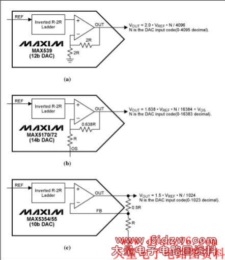
Figure 1. DAC output types: (a) fixed-gain without offset adjustment, (b) fixed-gain with offset adjustment, (c) force/sense.
The main advantage of the first two DAC types (Figure 1a and 1b) is the internal resistors are trimmed to provide typical gain error lower than ЁР1%, and they track each other closely over temperature to provide a typical gain tempco below 10ppm. The drawback is a single, fixed-gain that can only be changed by adding an amplifier after the DAC output. One advantage of the last two DAC types is the offset error can be removed with external circuitry. The force/sense type has a further advantage that specific gains can be set externally for a given application. The gain error for a force/sense DAC is specified in a unity-gain configuration (op amp output and inverting terminals connected), and additional gain error results from external resistor tolerances. The main drawback is that expensive discrete resistors, resistor arrays, or digital potentiometers are needed to match the gain tolerance and temperature drift characteristics of the fixed-gain DACs.
A final advantage of the force/sense DAC is it allows many useful circuits to be created with only a few simple external components. Several circuit examples are shown in the next section.
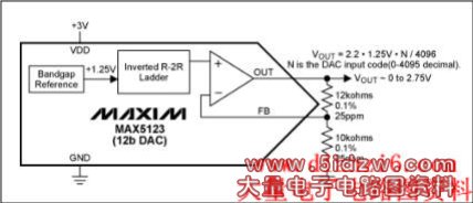
Figure 2. DAC with selectable fixed-gain of +2.20V/V.
Digitally programmable DAC gains are also possible by combining a force/sense DAC and digital potentiometer(s). Two examples of this using the MAX5175/MAX5177 DACs and MAX5400/MAX5415 digital potentiometers are shown in Figure 3. Both parts share the same SPI interface allowing write-only functionality to be implemented with four digital interface signals (clock, data input, and two chip selects).
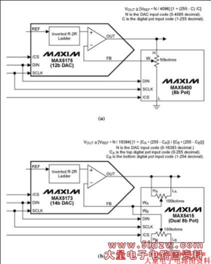
Figure 3. DAC with programmable gains using a digital potentiometer: (a) larger gain range, lower gain setting resolution, (b) smaller gain range, higher gain setting resolution.
In the first circuit (Figure 3a), the gain of the MAX5175 is set by a single MAX5400 digital potentiometer, defaulting to a gain of +1.992V/V at power-up. The gain tuning resolution is ~ЁР0.8% around this default value, indicating a gain of +2.00V/V can be set within ~ЁР0.4%. The non-linear gain range spans approximately +1V/V to +255V/V, although the upper usable gain will be limited by the reference and supply voltages. The gain setting resolution also worsens at higher gains. One big advantage of this circuit is the gain tempco will typically be ~5ppm/ЁуC since it is set by well-matched resistors inside a single potentiometer.
The second circuit (Figure 3b) uses a dual, 8-bit MAX5415 potentiometer to set the gain of a 14-bit, MAX5173 DAC. The power-up default gain of this circuit is exactly +2.00V, and the tuning resolution is <0.02% around this gain value. Because two 8-bit pots are used, this circuit has good tuning resolution over the entire non-linear gain range of 1 to 65. Although the resistance tempco between potentiometers is not specified, it should be close to the typical 5ppm/ЁуC ratiometric specification of the individual potentiometers since they both reside on the same silicon.
The circuits in Figure 3 provide the best of both worlds; gain setting flexibility of force/sense, as well as accurate gain (after trimming) and low temperature drift comparable to fixed-gain DACs.
Figures 4a and 4b show how the output op amp of a force/sense DAC can be configured as a transimpedance amplifier. In both examples, the current output from a photodiode is converted to a voltage by the transimpedance amplifier. In the first case, a single MAX5304 DAC is used to overcome its own offset voltage, and guarantee a slight reverse bias on a grounded photodiode. In the second, dual MAX5156/57 DACs are used to reverse or even zero bias the photodiode at any voltage level up to the reference voltage. One caution is that existing Maxim force/sense DACs have a maximum input bias current of 100nA on the FB pin (output op amp inverting input). This current may be too high for some photodiode applications, and an external op amp with lower input bias current such as the MAX4162 may be required until force/sense DACs with lower input bias currents become available. Another caution with the transimpedance amplifier topology is to confirm the op amp is stable, especially with capacitive loads at the inverting input.
ЃЌЪ§ФЃзЊЛЛЦїгІгУ-Force/Sense DAC Applic
Abstract: This article discusses application circuits for Maxim force/sense digital-to-analog converters (DACs). Applications include: selectable fixed-gain DAC, programmable gain DAC, photodiode bias control, amperometric sensor control, digitally programmable current source, Kelvin load sensing, temperature sensing, and high current DAC output. A brief description of the various DAC output configurations is also given.
Force/Sense DACs are unique because they provide user access to the inverting node of the output buffer amp in addition to the conventional output. These DACs are interesting because they provide flexibility to create custom DAC gains, or other useful circuits by simply adding a few simple components.
Types of Buffered, Voltage DAC Outputs
Figure 1 shows three common types of buffered, voltage output DACs. The first has a fixed-gain defined by an internal resistor ratio (typically +1.0, +1.638, or +2.0V/V), and no provision for adjusting the offset. The second type also uses internal resistors to set a fixed gain, but the normally grounded resistor tap in the non-inverting gain op amp topology is brought to an external pin allowing offset adjustment. The final output type is force/sense, which provides a pin connecting directly to the inverting terminal of the output op amp, yielding the most flexibility.Figure 1. DAC output types: (a) fixed-gain without offset adjustment, (b) fixed-gain with offset adjustment, (c) force/sense.
The main advantage of the first two DAC types (Figure 1a and 1b) is the internal resistors are trimmed to provide typical gain error lower than ЁР1%, and they track each other closely over temperature to provide a typical gain tempco below 10ppm. The drawback is a single, fixed-gain that can only be changed by adding an amplifier after the DAC output. One advantage of the last two DAC types is the offset error can be removed with external circuitry. The force/sense type has a further advantage that specific gains can be set externally for a given application. The gain error for a force/sense DAC is specified in a unity-gain configuration (op amp output and inverting terminals connected), and additional gain error results from external resistor tolerances. The main drawback is that expensive discrete resistors, resistor arrays, or digital potentiometers are needed to match the gain tolerance and temperature drift characteristics of the fixed-gain DACs.
A final advantage of the force/sense DAC is it allows many useful circuits to be created with only a few simple external components. Several circuit examples are shown in the next section.
Force/Sense DAC Application Circuits
An example of a custom, fixed-gain using the MAX5123's force/sense output is shown in Figure 2. In this example the internal +1.25V reference is used, and the gain is set to +2.20V/V with external discrete resistors to provide an approximate 0 to 2.75V DAC output voltage range.Figure 2. DAC with selectable fixed-gain of +2.20V/V.
Digitally programmable DAC gains are also possible by combining a force/sense DAC and digital potentiometer(s). Two examples of this using the MAX5175/MAX5177 DACs and MAX5400/MAX5415 digital potentiometers are shown in Figure 3. Both parts share the same SPI interface allowing write-only functionality to be implemented with four digital interface signals (clock, data input, and two chip selects).
Figure 3. DAC with programmable gains using a digital potentiometer: (a) larger gain range, lower gain setting resolution, (b) smaller gain range, higher gain setting resolution.
In the first circuit (Figure 3a), the gain of the MAX5175 is set by a single MAX5400 digital potentiometer, defaulting to a gain of +1.992V/V at power-up. The gain tuning resolution is ~ЁР0.8% around this default value, indicating a gain of +2.00V/V can be set within ~ЁР0.4%. The non-linear gain range spans approximately +1V/V to +255V/V, although the upper usable gain will be limited by the reference and supply voltages. The gain setting resolution also worsens at higher gains. One big advantage of this circuit is the gain tempco will typically be ~5ppm/ЁуC since it is set by well-matched resistors inside a single potentiometer.
The second circuit (Figure 3b) uses a dual, 8-bit MAX5415 potentiometer to set the gain of a 14-bit, MAX5173 DAC. The power-up default gain of this circuit is exactly +2.00V, and the tuning resolution is <0.02% around this gain value. Because two 8-bit pots are used, this circuit has good tuning resolution over the entire non-linear gain range of 1 to 65. Although the resistance tempco between potentiometers is not specified, it should be close to the typical 5ppm/ЁуC ratiometric specification of the individual potentiometers since they both reside on the same silicon.
The circuits in Figure 3 provide the best of both worlds; gain setting flexibility of force/sense, as well as accurate gain (after trimming) and low temperature drift comparable to fixed-gain DACs.
Figures 4a and 4b show how the output op amp of a force/sense DAC can be configured as a transimpedance amplifier. In both examples, the current output from a photodiode is converted to a voltage by the transimpedance amplifier. In the first case, a single MAX5304 DAC is used to overcome its own offset voltage, and guarantee a slight reverse bias on a grounded photodiode. In the second, dual MAX5156/57 DACs are used to reverse or even zero bias the photodiode at any voltage level up to the reference voltage. One caution is that existing Maxim force/sense DACs have a maximum input bias current of 100nA on the FB pin (output op amp inverting input). This current may be too high for some photodiode applications, and an external op amp with lower input bias current such as the MAX4162 may be required until force/sense DACs with lower input bias currents become available. Another caution with the transimpedance amplifier topology is to confirm the op amp is stable, especially with capacitive loads at the inverting input.
ЃЌЪ§ФЃзЊЛЛЦїгІгУ-Force/Sense DAC Applic
ЩЯвЛЦЊЃКA Smart Solid-State Fuse Cures