标签:高级电源管理,电源管理ic,电源管理软件,http://www.5idzw.com
A Smart Solid-State Fuse Cures,http://www.5idzw.com
The majority of asynchronous, inductor-based boost converters (the step-up switching types) exhibit a DC-current path between power source and load (Figure 1). This path can have two undesirable consequences: First, if a grounded output or other overload draws heavy output current for more than a few hundred milliseconds, the catch diode (usually a Schottky type) can exude that blended aroma of molten silicon and potting compound familiar to all true hackers. Second, if switching action is disabled for any reason, such as intentional shutdown, the load voltage remains just one diode drop below the supply voltage. The result can be indeterminate circuit behavior should this residual voltage be outside the load circuit's expected steady-state operating range.
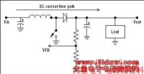
Figure 1. The problem of a direct path for current flow from source to load is intrinsic to the boost-converter topology.
Both problems are neatly solved for the relatively low output-current applications (<5A) that employ monolithic current-mode controllers and high-side current sensing. These circuits replace the catch diode with a synchronous switching transistor that can be disabled by shutdown or removal of input power. Disabling this internal transistor or turning it off during shutdown removes the path for DC current flow. The load then sees a requisite high-impedance disconnect. When not in shutdown, the circuit's cycle-by-cycle current-sensing mechanism (using an internal, high-side, current-sense resistor) protects against catastrophic meltdown from internal current overloads. Finally, thermal-overload protection provides a safe area of operation (SAO).
For applications with higher output current, in which pricing makes synchronous switching impractical for monolithic devices, the load-disconnect function requires a high-side switch external to the controller die. A discrete current-mode topology using a high-side current-sense resistor and a synchronous switching transistor is possible, but that approach suffers from PC-board parasitics and layout dependencies, especially at high switching frequencies. The result is a relatively complex design, particularly when system constraints mandate a low input voltage (<3.6V).
A synchronous, high-side external switch becomes feasible at higher levels of peak inductor current (>5A), but cost and complexity override heat and efficiency considerations at the more moderate levels of inductor current (~1.5A to 5A) discussed in this article. A simple catch diode is again the most desirable solution. The challenge is to achieve the desired load disconnect while retaining use of the humble catch diode and the unadorned boost topology.
A simple and smart solution is presented in Figure 2, where a MAX668 controller illustrates the demanding task of boosting from low input voltages. This current-mode boost controller drives a logic-level n-channel enhancement-mode MOSFET (configured on the low side) in series with a low-side current-sense resistor; neither is shown in Figure 2. Instead, this circuitry and the MAX668 are represented as a block to avoid cluttering the load connect/disconnect function. The high-side switch is a Schottky catch diode chosen for its low forward-voltage drop (now standard). The simple boost topology remains intact. This application boosts 3.3V to 5V and delivers load currents to 3A. The MAX668 boosts only from 3V or higher, but the MAX669 can accept inputs as low as 1.8V.
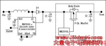
Figure 2. This boost converter with load disconnect illustrates the minimum-cost configuration.
The key element in implementing a smart load disconnect is the p-channel enhancement-mode MOSFET Q1. As shown, the system can enable this boost circuit (active-low ON ) or shut it down (OFF). D1 conducts during shutdown, producing 3.3V minus one diode drop at the MAX810L supply terminal. (This tiny power-on-reset device has a SOT23-3 package, draws about 24µA quiescent current, and guarantees operation at 1V.) In this case the MAX810L output is high, because its nominal reset threshold is 4.65V, which forces Q1 off and disconnects the load from the main supply.
The MAX668 feedback resistors are set to produce a 5V output when that device exits shutdown. When the rising output exceeds the MAX810L input threshold, an internal one-shot turns on for approximately 240msec. After this timeout period, the MAX810 output goes low and turns Q1 on.
When Q1 is on, the MAX810 constantly monitors the supply line for overload currents. An overload causes the output to sag below the MAX810's internal threshold voltage, making its output go high with a nominal 20usec delay, turning off Q1, and disconnecting the load. Soon after, the MAX668 boosting action raises the MAX810 input voltage above its threshold. After timeout, the MAX810 reconnects the load automatically. This cycle repeats until the excessive load is removed or the boost circuit is disabled. Thus, Q1 and the MAX810 act as a smart solid-state switch.
The MAX810 (a micropower device) has a rather wimpy push-pull output stage. It resembles a ~6KΩ resistor when sourcing current and a ~125Ω resistor when sinking current. When the device turns off or on, these resistances slow things down by acting against Q1's Miller capacitance and the associated Cgs. The associated RC time constant for a large pass transistor is ~0.6µs, if we assume a total effective capacitance of 5000pF acting against the MAX810's 125Ω sinking stage. Thus, a full voltage transition can be approximated as 10RC = 6µs.
Turning the same device fully off requires nearly 48 times' longer (6K/125 at 290µs). This approximation is workable, but actual turn-off occurs when VOUT reaches the enhancement threshold voltage (Vth), well before 10 times' constants elapse. Turn-off time is quite acceptable with the Q1/MAX810 combination acting as a solid-state fuse. On the other hand, turn-on time can be a problem, depending on the startup load and the pass transistor's ratio of source bypass to drain bypass capacitances. If the startup load is small and C1 is large compared to C2, then a quick FET turn-on causes only a small voltage dip at the MAX810 input (less than that required to trigger a reset). For these conditions, the least expensive implementation of this circuit topology is that shown in Figure 2.
,A Smart Solid-State Fuse Cures
The majority of asynchronous, inductor-based boost converters (the step-up switching types) exhibit a DC-current path between power source and load (Figure 1). This path can have two undesirable consequences: First, if a grounded output or other overload draws heavy output current for more than a few hundred milliseconds, the catch diode (usually a Schottky type) can exude that blended aroma of molten silicon and potting compound familiar to all true hackers. Second, if switching action is disabled for any reason, such as intentional shutdown, the load voltage remains just one diode drop below the supply voltage. The result can be indeterminate circuit behavior should this residual voltage be outside the load circuit's expected steady-state operating range.
Figure 1. The problem of a direct path for current flow from source to load is intrinsic to the boost-converter topology.
Both problems are neatly solved for the relatively low output-current applications (<5A) that employ monolithic current-mode controllers and high-side current sensing. These circuits replace the catch diode with a synchronous switching transistor that can be disabled by shutdown or removal of input power. Disabling this internal transistor or turning it off during shutdown removes the path for DC current flow. The load then sees a requisite high-impedance disconnect. When not in shutdown, the circuit's cycle-by-cycle current-sensing mechanism (using an internal, high-side, current-sense resistor) protects against catastrophic meltdown from internal current overloads. Finally, thermal-overload protection provides a safe area of operation (SAO).
For applications with higher output current, in which pricing makes synchronous switching impractical for monolithic devices, the load-disconnect function requires a high-side switch external to the controller die. A discrete current-mode topology using a high-side current-sense resistor and a synchronous switching transistor is possible, but that approach suffers from PC-board parasitics and layout dependencies, especially at high switching frequencies. The result is a relatively complex design, particularly when system constraints mandate a low input voltage (<3.6V).
A synchronous, high-side external switch becomes feasible at higher levels of peak inductor current (>5A), but cost and complexity override heat and efficiency considerations at the more moderate levels of inductor current (~1.5A to 5A) discussed in this article. A simple catch diode is again the most desirable solution. The challenge is to achieve the desired load disconnect while retaining use of the humble catch diode and the unadorned boost topology.
A simple and smart solution is presented in Figure 2, where a MAX668 controller illustrates the demanding task of boosting from low input voltages. This current-mode boost controller drives a logic-level n-channel enhancement-mode MOSFET (configured on the low side) in series with a low-side current-sense resistor; neither is shown in Figure 2. Instead, this circuitry and the MAX668 are represented as a block to avoid cluttering the load connect/disconnect function. The high-side switch is a Schottky catch diode chosen for its low forward-voltage drop (now standard). The simple boost topology remains intact. This application boosts 3.3V to 5V and delivers load currents to 3A. The MAX668 boosts only from 3V or higher, but the MAX669 can accept inputs as low as 1.8V.
Figure 2. This boost converter with load disconnect illustrates the minimum-cost configuration.
The key element in implementing a smart load disconnect is the p-channel enhancement-mode MOSFET Q1. As shown, the system can enable this boost circuit (active-low ON ) or shut it down (OFF). D1 conducts during shutdown, producing 3.3V minus one diode drop at the MAX810L supply terminal. (This tiny power-on-reset device has a SOT23-3 package, draws about 24µA quiescent current, and guarantees operation at 1V.) In this case the MAX810L output is high, because its nominal reset threshold is 4.65V, which forces Q1 off and disconnects the load from the main supply.
The MAX668 feedback resistors are set to produce a 5V output when that device exits shutdown. When the rising output exceeds the MAX810L input threshold, an internal one-shot turns on for approximately 240msec. After this timeout period, the MAX810 output goes low and turns Q1 on.
When Q1 is on, the MAX810 constantly monitors the supply line for overload currents. An overload causes the output to sag below the MAX810's internal threshold voltage, making its output go high with a nominal 20usec delay, turning off Q1, and disconnecting the load. Soon after, the MAX668 boosting action raises the MAX810 input voltage above its threshold. After timeout, the MAX810 reconnects the load automatically. This cycle repeats until the excessive load is removed or the boost circuit is disabled. Thus, Q1 and the MAX810 act as a smart solid-state switch.
The MAX810 (a micropower device) has a rather wimpy push-pull output stage. It resembles a ~6KΩ resistor when sourcing current and a ~125Ω resistor when sinking current. When the device turns off or on, these resistances slow things down by acting against Q1's Miller capacitance and the associated Cgs. The associated RC time constant for a large pass transistor is ~0.6µs, if we assume a total effective capacitance of 5000pF acting against the MAX810's 125Ω sinking stage. Thus, a full voltage transition can be approximated as 10RC = 6µs.
Turning the same device fully off requires nearly 48 times' longer (6K/125 at 290µs). This approximation is workable, but actual turn-off occurs when VOUT reaches the enhancement threshold voltage (Vth), well before 10 times' constants elapse. Turn-off time is quite acceptable with the Q1/MAX810 combination acting as a solid-state fuse. On the other hand, turn-on time can be a problem, depending on the startup load and the pass transistor's ratio of source bypass to drain bypass capacitances. If the startup load is small and C1 is large compared to C2, then a quick FET turn-on causes only a small voltage dip at the MAX810 input (less than that required to trigger a reset). For these conditions, the least expensive implementation of this circuit topology is that shown in Figure 2.
,A Smart Solid-State Fuse Cures