БъЧЉЃКИпМЖЕчдДЙмРэ,ЕчдДЙмРэic,ЕчдДЙмРэШэМў,http://www.5idzw.com
Ъ§ФЃзЊЛЛЦїгІгУ-Force/Sense DAC Applic,http://www.5idzw.com
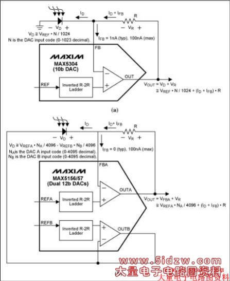
Figure 4. Bias voltage control of a photodiode and transimpedance amplifier: (a) grounded reverse bias with single DAC, (b) level shifted zero or reverse bias with dual DACs.
Another transimpedance application is shown in Figure 5. In this example, the DAC provides a DC voltage bias for an amperometric sensor, and the sensor's output current is converted to a voltage by the DAC's transimpedance amplifier. Amperometric (or more generally voltammetric) sensors are commonly used in medical applications, and the force/sense DAC is a natural fit.
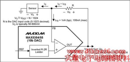
Figure 5. Voltage bias control for an amperometric sensor.
A force/sense DAC can also be configured as a digitally programmable current source (actually a sink) using the topology shown in Figure 6. Assuming the DAC output has enough headroom to drive the ~0.7V base-emitter voltage of the NPN BJT, feedback will hold the voltage across the resistor (and hence its current) constant at the unbuffered R-2R ladder output voltage(VR2R). The output current at the BJT's collector will be slightly lower than the programmed resistor current due to the BJT's finite beta. This may require calibration of the output current in some applications. One remedy is to use a MOSFET in place of the BJT since its drain current is virtually equal to its source current at DC or low frequencies.
Common uses for this circuit include general-purpose current sources, precise LED drive current, and 4-20mA current loops in industrial control applications.
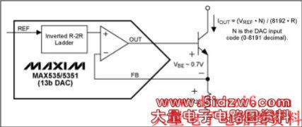
Figure 6. Digitally programmable current source.
By using Kelvin sensing, force/sense DACs are able to deliver a desired voltage at the load, even if the series impedance between the DAC output and load is relatively high. Once again, this assumes the DAC output has enough headroom to drive the divider formed by the series and load impedances. The user should confirm the output op amp is stable for all expected impedance values in the feedback loop.
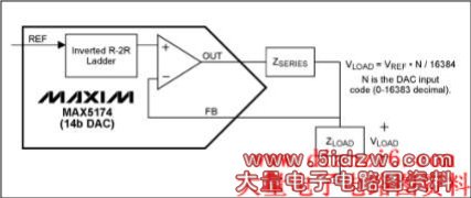
Figure 7. Driven signal with kelvin sensing at load.
Several products are now available that use discrete diode or transistor P-N junctions for remote temperature sensing. These devices use ratios of 2 (or more) currents along with the diode equation to determine the temperature in Kelvin.
Figure 8 shows a simple circuit topology where a MAX5302 DAC is used to drive a diode-connected transistor. Currents (1023 possible values) are set by the DAC output voltage across the grounded resistor (VR/R), and the resulting forward-biased, P-N junction voltage (VD) is measured differentially using a MAX1408 ADC. This topology is convenient because the same resistor is used to set both currents, and the current ratios are approximately the ratios of DAC code words. For example, DAC codes of 1000 (decimal) and 500 (decimal) produce a current ratio of 2:1 that can be used directly in the diode equation calculations. There will be a few DAC error terms such as offset, INL, and gain affecting the ratio, but these will be relatively minor. If more accuracy is needed, the precise current ratio can be determined by using the ADC to measure the forced resistor voltage (VR) at each DAC code. Care should be taken with this circuit to ensure op amp stability, especially for distant P-N junctions with long leads and large parasitics.
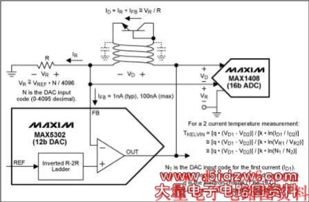
Figure 8. Diode current drive for temperature sensing.
The final application circuit shown in Figure 9 is a MAX5352/53 force/sense DAC with an emitter-follower, BJT stage to increase output current drive. This topology is similar to the current source shown in Figure 6, except the collector is tied to VCC (common-collector) and the output is a voltage at the emitter rather than current at the collector. As with many previous circuits, a key requirement is that the DAC output have enough headroom to drive the BJT's base-emitter junction ~0.7V above the maximum output voltage.
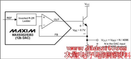
Figure 9. Increased DAC output current drive with an emitter-follower.
Table 1. Maxim Force/Sense DACs
Figure 4. Bias voltage control of a photodiode and transimpedance amplifier: (a) grounded reverse bias with single DAC, (b) level shifted zero or reverse bias with dual DACs.
Another transimpedance application is shown in Figure 5. In this example, the DAC provides a DC voltage bias for an amperometric sensor, and the sensor's output current is converted to a voltage by the DAC's transimpedance amplifier. Amperometric (or more generally voltammetric) sensors are commonly used in medical applications, and the force/sense DAC is a natural fit.
Figure 5. Voltage bias control for an amperometric sensor.
A force/sense DAC can also be configured as a digitally programmable current source (actually a sink) using the topology shown in Figure 6. Assuming the DAC output has enough headroom to drive the ~0.7V base-emitter voltage of the NPN BJT, feedback will hold the voltage across the resistor (and hence its current) constant at the unbuffered R-2R ladder output voltage(VR2R). The output current at the BJT's collector will be slightly lower than the programmed resistor current due to the BJT's finite beta. This may require calibration of the output current in some applications. One remedy is to use a MOSFET in place of the BJT since its drain current is virtually equal to its source current at DC or low frequencies.
Common uses for this circuit include general-purpose current sources, precise LED drive current, and 4-20mA current loops in industrial control applications.
Figure 6. Digitally programmable current source.
By using Kelvin sensing, force/sense DACs are able to deliver a desired voltage at the load, even if the series impedance between the DAC output and load is relatively high. Once again, this assumes the DAC output has enough headroom to drive the divider formed by the series and load impedances. The user should confirm the output op amp is stable for all expected impedance values in the feedback loop.
Figure 7. Driven signal with kelvin sensing at load.
Several products are now available that use discrete diode or transistor P-N junctions for remote temperature sensing. These devices use ratios of 2 (or more) currents along with the diode equation to determine the temperature in Kelvin.
Figure 8 shows a simple circuit topology where a MAX5302 DAC is used to drive a diode-connected transistor. Currents (1023 possible values) are set by the DAC output voltage across the grounded resistor (VR/R), and the resulting forward-biased, P-N junction voltage (VD) is measured differentially using a MAX1408 ADC. This topology is convenient because the same resistor is used to set both currents, and the current ratios are approximately the ratios of DAC code words. For example, DAC codes of 1000 (decimal) and 500 (decimal) produce a current ratio of 2:1 that can be used directly in the diode equation calculations. There will be a few DAC error terms such as offset, INL, and gain affecting the ratio, but these will be relatively minor. If more accuracy is needed, the precise current ratio can be determined by using the ADC to measure the forced resistor voltage (VR) at each DAC code. Care should be taken with this circuit to ensure op amp stability, especially for distant P-N junctions with long leads and large parasitics.
Figure 8. Diode current drive for temperature sensing.
The final application circuit shown in Figure 9 is a MAX5352/53 force/sense DAC with an emitter-follower, BJT stage to increase output current drive. This topology is similar to the current source shown in Figure 6, except the collector is tied to VCC (common-collector) and the output is a voltage at the emitter rather than current at the collector. As with many previous circuits, a key requirement is that the DAC output have enough headroom to drive the BJT's base-emitter junction ~0.7V above the maximum output voltage.
Figure 9. Increased DAC output current drive with an emitter-follower.
Maxim Force/Sense DACs
Table 1 lists all of the force/sense DACs currently offered by Maxim. A few key specifications are also shown.Table 1. Maxim Force/Sense DACs
|
|
|
|
|
Reference | |||
|
|
|
|
|
Ext., 0 to VDD-1.4V | |||
| MAX5354 | Single | 10 Bits | 4.5V to 5.5V | Ext., 0 to VDD-1.4V | |||
| MAX5355 | Single | 10 Bits | 3.15V to 3.6V | Ext., 0 to VDD-1.4V | |||
| MAX5250 | Quad | 10 Bits | 4.5V to 5.5V | 2 Ext., 0 to VDD-1.4V | |||
| MAX5251 | Quad | 10 Bits | 3.0V to 3.6V | 2 Ext., 0 to VDD-1.4V | |||
| MAX5302 | Single | 12 Bits | 4.5V to 5.5V | Ext., 0 to VDD-1.4V | |||
| MAX5175 | Single | 12 Bits | 4.5V to 5.5V | Ext., 0 to VDD-1.4V | |||
| MAX5177 | Single | 12 Bits | 2.7V to 3.6V | Ext., 0 to VDD-1.4V | |||
| MAX5352 | Single | 12 Bits | 4.5V to 5.5V | Ext., 0 to VDD-1.4V | |||
| MAX5353 | Single | 12 Bits | 3.15V to 3.6V | Ext., 0 to VDD-1.4V | |||
| MAX5122 | Single | 12 Bits | 4.5V to 5.5V | Int., 2.5V, 10ppm | |||
| MAX5123 | Single | 12 Bits | 2.7V to 3.6V | Int., 1.25V, 10ppm | |||
| MAX5156 | Dual | 12 Bits | 4.5V to 5.5V | 2 Ext., 0 to VDD-1.4V | |||
| MAX5157 | Dual | 12 Bits | 2.7V to 3.6V | 2 Ext., 0 to VDD-1.4V | |||
| MAX525 | Quad | 12 Bits | 4.5V to 5.5V | 2 Ext., 0 to VDD-1.4V | |||
| MAX5253 | Quad | 12 Bits | 3.0V to 3.6V | 2 Ext., 0 to VDD-1.4V | |||
| MAX535 | Single | 13 Bits | 4.5V to 5.5V | Ext., 0 to VDD-1.4V | |||
| MAX5351 | Single | 13 Bits | 3.15V to 3.6V | Ext., 0 to VDD-1.4V | |||
| MAX5132 | Single | 13 Bits | 4.5V to 5.5V | Int., 2.5V, 10ppm | |||
| MAX5133 | Single | 13 Bits | 2.7V to 3.6V | Int., 1.25V, 10ppm | |||
| MAX5152 | Dual | 13 Bits | 4.5V to 5.5V | 2 Ext., 0 to VDD-1.4V | |||
| MAX5153 | Dual | 13 Bits | 2.7V to 3.6V | 2 Ext., 0 to VDD-1.4V | |||
| MAX5171 | Single | 14 Bits | 4.5V to 5.5V | Ext., 0 to VDD-1.4V | |||
| MAX5173 | Single | 14 Bits | 2.7V to 3.6V | Ext., 0 to VDD-1.4V | |||
<-- END: DB HTML -->
ЩЯвЛЦЊЃКA Smart Solid-State Fuse Cures