标签:模拟电子技术基础,模拟电子电路,http://www.5idzw.com
Reference Voltage for Multiple,http://www.5idzw.com
Abstract: This paper discusses the successful implementation of two reference circuits tailored to the space-saving needs of ultrasound imaging applications, which commonly encounter the demand for one reference source to power multiple analog-to-digital converters (ADCs). Finally, the two circuits were put to the test and their results are discussed in the following note.
The achievable accuracy for systems with multiple analog-to-digital converters (ADCs) depends directly on the reference voltage(s) applied to the ADCs. Medical ultrasound imaging systems, for example, commonly include a large number of ADCs in the receiver's beamformer electronics, usually organized in groups of 16, 24, 32, etc. Maximum beam accuracy requires that you minimize errors in this path. Poor accuracy in the reference voltage of individual ADCs degrades the overall system, as does the distributed load, which consists of many individual resistive and capacitive loads. Several approaches can provide the reference voltage for such ADC arrays:
An ADC's noise level determines its useable dynamic range; this dynamic range should generally be as large as possible. The reference noise component of ADC noise can be additive or multiplicative. Additive noise is easily filtered by local bypass capacitors on the individual ADCs, which in most designs are already present to optimize the ADC's dynamic performance.
Multiplicative noise, on the other hand, is more insidious. For ultrasound applications, reference noise in the audio frequency spectrum can modulate large "stationary" signals in the RF spectrum. Such signals are produced by stationary tissue in the ultrasound target. Audio modulation produces sidebands on the RF signal that can be demodulated by a Doppler detector, producing audio tones in the detected Doppler output signal.
To estimate the amount of audio noise tolerable in an ultrasound application, assume a nearly full-scale RF signal applied to a 10-bit ADC like the MAX1448. The dynamic range of that device (almost 60dB) implies a noise floor of -60dBFS. That noise level can be normalized to a 1Hz bandwidth. The Nyquist bandwidth for 80MHz sampling rate would be 40MHz. The correction factor is √(40MHz)= 76dB, which places the ADC's noise floor at -60dBFS - 76dBFS = -136dBFS. Because a conservative design requires the reference voltage noise to be at least 20dB lower (-156dBFS), a +2.0V reference requires an extremely low noise level of 33nVP-P (approximately 8nVRMS/√ Hz).
An array with multiple ADCs may require a reference voltage more accurate than that internal to each converter (the reference internal to MAX144x converters, for example, is ±1% accurate). The following two circuits are submitted as reference designs for such arrays. They feature a single common low-frequency noise filter, and they achieve high-frequency noise suppression with local decoupling capacitors on individual ADCs.
A precision source like the MAX6062 (IC1) generates an external DC level of +2.048V (Figure 1), and exhibits a noise voltage density of 150nV/√Hz. Its output passes through a 1-pole lowpass filter (with 10Hz cutoff frequency) to an op amp (IC2), such as the MAX4250, which buffers the reference before its output is applied to a second 10Hz lowpass filter. IC2 (MAX4250) provides a low offset voltage (for high gain accuracy) and a low noise level. The passive 10Hz filter following the buffer attenuates noise produced in the voltage reference and buffer stages. This filtered noise density, which decreases for higherfrequencies, meets the noise levels specified for precise ADC operation.
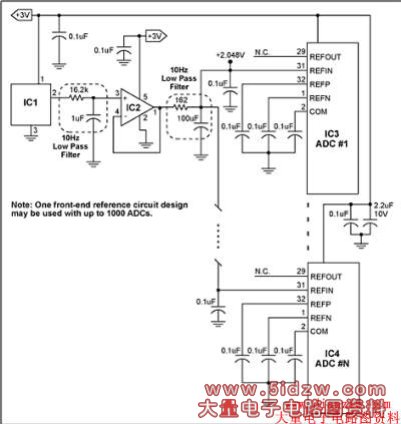
Figure 1. For ultrasound applications, a single low-noise reference circuit drives up to 1000 ADCs.
The converters of the MAX144x family are specified for a typical gain error of ±4.4% (better than ±0.5dB). This performance is better than the gain tolerance of all other building blocks in the signal path of an ultrasound receiver. Note that proper power-up/-down sequencing is ensured because all active parts are driven from the same supply voltage. This approach yields excellent gain matching and a very low noise level with minimal circuitry, and should suffice in many applications that require multiple gain-matched ADCs.
,Reference Voltage for Multiple
Abstract: This paper discusses the successful implementation of two reference circuits tailored to the space-saving needs of ultrasound imaging applications, which commonly encounter the demand for one reference source to power multiple analog-to-digital converters (ADCs). Finally, the two circuits were put to the test and their results are discussed in the following note.
The achievable accuracy for systems with multiple analog-to-digital converters (ADCs) depends directly on the reference voltage(s) applied to the ADCs. Medical ultrasound imaging systems, for example, commonly include a large number of ADCs in the receiver's beamformer electronics, usually organized in groups of 16, 24, 32, etc. Maximum beam accuracy requires that you minimize errors in this path. Poor accuracy in the reference voltage of individual ADCs degrades the overall system, as does the distributed load, which consists of many individual resistive and capacitive loads. Several approaches can provide the reference voltage for such ADC arrays:
- Individual on-chip references: Though it offers a convenient connection locally to each ADC, this option features relatively poor matching between the converters.
- A single external reference voltage applied to all reference inputs of the ADC array: Such a configuration lets you engineer an external reference voltage of arbitrary accuracy, but incurs error due to small variations among the resistor ladders (one ladder internal to each ADC).
- An external reference driving the ADCs' reference ladder taps directly: This option delivers maximum gain accuracy by directly controlling the reference voltage applied to each ADC ladder. However, it requires driving the (relatively) low resistance of the ladders, and some ADCs do not allow access to that internal bias point.
ADC Accuracy
For many applications, gain and noise level have a major effect on ADC accuracy. The gain of an ADC is represented by the slope of its transfer function, which relates analog inputs to the allowable range of digital output codes. One way to quantify gain is to measure the full-scale (FS) input range, which is directly controlled by the reference voltage level. For medical ultrasound imaging systems, variation in the full-scale range of the ADCs can cause errors in beam formation. This also varies the ADCs' clipping point―an effect that may be important in certain signal demodulation schemes.An ADC's noise level determines its useable dynamic range; this dynamic range should generally be as large as possible. The reference noise component of ADC noise can be additive or multiplicative. Additive noise is easily filtered by local bypass capacitors on the individual ADCs, which in most designs are already present to optimize the ADC's dynamic performance.
Multiplicative noise, on the other hand, is more insidious. For ultrasound applications, reference noise in the audio frequency spectrum can modulate large "stationary" signals in the RF spectrum. Such signals are produced by stationary tissue in the ultrasound target. Audio modulation produces sidebands on the RF signal that can be demodulated by a Doppler detector, producing audio tones in the detected Doppler output signal.
To estimate the amount of audio noise tolerable in an ultrasound application, assume a nearly full-scale RF signal applied to a 10-bit ADC like the MAX1448. The dynamic range of that device (almost 60dB) implies a noise floor of -60dBFS. That noise level can be normalized to a 1Hz bandwidth. The Nyquist bandwidth for 80MHz sampling rate would be 40MHz. The correction factor is √(40MHz)= 76dB, which places the ADC's noise floor at -60dBFS - 76dBFS = -136dBFS. Because a conservative design requires the reference voltage noise to be at least 20dB lower (-156dBFS), a +2.0V reference requires an extremely low noise level of 33nVP-P (approximately 8nVRMS/√ Hz).
An array with multiple ADCs may require a reference voltage more accurate than that internal to each converter (the reference internal to MAX144x converters, for example, is ±1% accurate). The following two circuits are submitted as reference designs for such arrays. They feature a single common low-frequency noise filter, and they achieve high-frequency noise suppression with local decoupling capacitors on individual ADCs.
Single External Reference
Multiple-converter systems based on the MAX144x family are well suited for use with a common reference voltage. The REFIN pin of those converters can be connected directly to an external reference source, eliminating the need for any circuit modification. Moreover, the high input impedance of REFIN (even of multiple REFIN terminals connected in parallel) draws only a small load current.A precision source like the MAX6062 (IC1) generates an external DC level of +2.048V (Figure 1), and exhibits a noise voltage density of 150nV/√Hz. Its output passes through a 1-pole lowpass filter (with 10Hz cutoff frequency) to an op amp (IC2), such as the MAX4250, which buffers the reference before its output is applied to a second 10Hz lowpass filter. IC2 (MAX4250) provides a low offset voltage (for high gain accuracy) and a low noise level. The passive 10Hz filter following the buffer attenuates noise produced in the voltage reference and buffer stages. This filtered noise density, which decreases for higherfrequencies, meets the noise levels specified for precise ADC operation.
Figure 1. For ultrasound applications, a single low-noise reference circuit drives up to 1000 ADCs.
The converters of the MAX144x family are specified for a typical gain error of ±4.4% (better than ±0.5dB). This performance is better than the gain tolerance of all other building blocks in the signal path of an ultrasound receiver. Note that proper power-up/-down sequencing is ensured because all active parts are driven from the same supply voltage. This approach yields excellent gain matching and a very low noise level with minimal circuitry, and should suffice in many applications that require multiple gain-matched ADCs.
Generating a Precision External Reference
For applications requiring more stringent gain matching (Figure 2), the MAX144x family again is well suited. Connecting each REFIN to analog ground disables the internal reference of each device, allowing the internal reference ladders to be driven directly by a set of external reference sources. These voltages can have an arbitrarily tight tolerance, and the ADCs track them typically within 0.1%. ADCs of this family also feature a 4kΩ resistance across the ladder reference connection, which allows the load to be easily driven even if many ADCs are operated in parallel.,Reference Voltage for Multiple