标签:模拟电子技术基础,模拟电子电路,http://www.5idzw.com
Minimize Voltage Offsets in Pr,http://www.5idzw.com
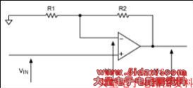
Figure 1. This simplified schematic depicts an ideal op-amp circuit.
The analysis of this circuit should be well known to first-year students (we assume zero current at the amplifier inputs):
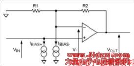
Figure 2. Current sources model input bias currents for the ideal op amp of Figure 1.
To analyze the effect of each of these current sources, assume that VIN = 0V. We assume that the impedance at VIN is small in relation to other impedances, so IBIAS+ will be shunted to ground and have no effect. Because VIN = 0V, V- must also equal 0V. Moreover, because both ends of R1 are at the same 0V potential, it can be eliminated from the analysis. Thus, we immediately see an unwanted output offset (VOUT), due to the input bias current (IBIAS-) and feedback resistor (R2):
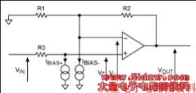
Figure 3. Adding a compensation resistor (R3) to the Figure 2 circuit cancels the effect of input bias currents.
With VIN = 0, you can easily calculate VOUT by noting that we have a voltage adder circuit, i.e., the output voltage is the voltage applied to the positive terminal times the voltage gain, plus an offset due to input current leakage into the negative terminal. Because VIN = 0, any voltage applied to the positive terminal is due to leakage into that terminal, and R3:
Data sheets for these devices show that they exhibit constant resistance at the resistor-pair node for resistor ratios of 2, 4, and 8. If the ratio is 1, you see only the low resistance of the node. For all ratios, therefore, the matching resistor should equal the wiper resistance (Table 1).
Table 1. Matching Resistor Settings for MAX5421/MAX5431 Dividers
Resistor tolerances are shown in Table 2.
Table 2. Resistor Tolerances for MAX5421/MAX5431 Dividers
,Minimize Voltage Offsets in Pr
Minimize Voltage Offsets in Precision Amplifiers
Abstract: Voltage-offset errors in precision amplifiers are partly caused by input bias currents. This article analyzes the problem and proposes a solution based on resistor networks, both discrete and integrated. The analysis shows that integrated resistors can outperform the more costly discrete approach.
In precision electronics, amplifier stages must comply with precisely designed performance specifications. One problem encountered when designing these amplifiers is the voltage offset generated by currents flowing into the amplifier inputs. In this article, we first analyze the source of this offset, and then propose a solution based on integrated resistor networks.
Analyzing the Problem
Before attempting to solve a problem, we need to understand its source. For that purpose, consider the simplified schematic for an ideal op amp (Figure 1).Figure 1. This simplified schematic depicts an ideal op-amp circuit.
The analysis of this circuit should be well known to first-year students (we assume zero current at the amplifier inputs):
Rearranging: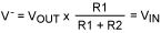
You can make the analysis more realistic by introducing a finite input resistance, which gives the op amp a finite input bias current. We model this effect with a current source on each input of the ideal op amp (Figure 2).
Figure 2. Current sources model input bias currents for the ideal op amp of Figure 1.
To analyze the effect of each of these current sources, assume that VIN = 0V. We assume that the impedance at VIN is small in relation to other impedances, so IBIAS+ will be shunted to ground and have no effect. Because VIN = 0V, V- must also equal 0V. Moreover, because both ends of R1 are at the same 0V potential, it can be eliminated from the analysis. Thus, we immediately see an unwanted output offset (VOUT), due to the input bias current (IBIAS-) and feedback resistor (R2):
VOUT = IBIAS- × R2
Solving the Problem
The circuit can be improved by adding one extra resistor (R3 in Figure 3). We need to examine the effect of this extra resistor, which causes the positive input to be offset negative by IBIAS+ × R3. You can, therefore, adjust R3 to nullify the effect of bias current into the negative input. It is reasonable, however, to make the approximation that positive and negative input bias currents are the same.Figure 3. Adding a compensation resistor (R3) to the Figure 2 circuit cancels the effect of input bias currents.
With VIN = 0, you can easily calculate VOUT by noting that we have a voltage adder circuit, i.e., the output voltage is the voltage applied to the positive terminal times the voltage gain, plus an offset due to input current leakage into the negative terminal. Because VIN = 0, any voltage applied to the positive terminal is due to leakage into that terminal, and R3:
If R3 equals the parallel combination of R1 and R2, the voltages generated by input bias currents should cancel. For the high-precision applications in which this technique is generally used, the resistors should be specified as follows:
- The ratio R2/R1 must have high precision in order to set a precision gain.
- The match between R3 and the parallel combination of R1 and R2 must also be high precision so errors introduced by the input bias currents are compensated.
- These resistors must track with temperature.
Integrated Resistors
The MAX5421 (as an example) includes 15kΩ resistors and operates with a supply voltage of +5V or -5V. A similar part, the MAX5431, includes 57kΩ resistors and operates with a supply voltage of +15V or -15V. These devices not only include precision integrated resistors, but they also switch between the resistors. When the resistors are used to set gain in an op-amp circuit, this capability allows you to choose among programmable gains of 1, 2, 4, and 8.Data sheets for these devices show that they exhibit constant resistance at the resistor-pair node for resistor ratios of 2, 4, and 8. If the ratio is 1, you see only the low resistance of the node. For all ratios, therefore, the matching resistor should equal the wiper resistance (Table 1).
Table 1. Matching Resistor Settings for MAX5421/MAX5431 Dividers
| MAX5421 (VDD = +5V, VSS = -5V) |
MAX5431 (VDD = +15V, VSS = -15V) | ||
| Wiper Resistance (kΩ, typ) | Rati 1 | 0.3 | 0.5 |
| Rati 2, 4, 8 | 8 | 14 | |
| Matching Resistance (kΩ, typ) | Rati 1 | 0.3 | 0.5 |
| Rati 2, 4, 8 | 8 | 14 | |
Resistor tolerances are shown in Table 2.
Table 2. Resistor Tolerances for MAX5421/MAX5431 Dividers
| Part | Divider Ratio Accuracy (±%, max) |
| MAX5421_A | 0.025 |
| MAX5421_B | 0.09 |
| MAX5421_C | 0.5 |
| MAX5431_A | 0.025 |
| MAX5431_B | 0.09 |
| MAX5431_C | 0.5 |