标签:高级电源管理,电源管理ic,电源管理软件,http://www.5idzw.com
A Smart Solid-State Fuse Cures,http://www.5idzw.com
If the external load or the charging of C2 draws a heavy current at startup, such that a fast turn-on of Q1 could cause the MAX810 to issue a reset, an RC network can be added to slow the turn-on (Figure 3). A proper selection of these components can apply the load over multiple switching cycles of the MAX668, enabling its output voltage to remain above the reset threshold. Slowing the Q1 turn-on may be desirable, but slowing the turn-off may not be. Accordingly, the circuit includes a Schottky diode in parallel with the resistor to disable Q1 quickly in response to an excessive and unexpected load.
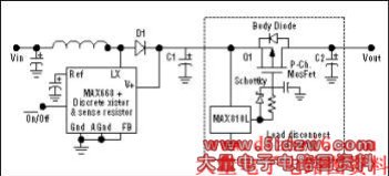
Figure 3. Adding three components in the MOSFET-gate circuit of Figure 2 provides the slow-connect/fast-disconnect necessary to accommodate heavy startup loads.
These circuits require a logic-level p-channel MOSFET such as Q1 to fully enhance the channel and obtain a low Rds-on. If Q1's on-resistance is high enough to cause a significant voltage drop (especially in low-output-voltage applications, or if the load is relatively far away), then it can be desirable to regulate the drain side of Q1. In doing this, you should minimize parasitics and observe good circuit-layout techniques. This remote regulation can be implemented with a SPDT, low-voltage analog switch in a SOT23 package (MAX4544), controlled by the MAX810's output state (Figure 4).
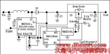
Figure 4. Further embellishments (to Figure 3) add remote-sense regulation and low-voltage detection to the boost converter with load disconnect.
The MAX4544 operates within data-sheet limits for supply voltages as low as 2.7V. With the input supply at 3.3V and about 0.3V across the Schottky diode, the MAX4544 (and MAX810) remains operational even when the boost converter is shut down. The MAX810 output is high during shutdown, connecting the MAX4544 COM node to NO (the Q1 source). When the boost converter turns on, resistors connected to the MAX4544 COM pin provide feedback to the MAX668. MAX4544 on-resistance is 60Ω maximum with a 5V supply, so the feedback-resistor values should be much larger than that to minimize output-voltage errors. On-resistance is only 120Ω at 3V; thus, the MAX4544 switch errors are minimal even for lower output voltages.
When the boost circuit is enabled and after the timeout period has elapsed, the MAX810 output goes low and connects the load by means of Q1. Simultaneously, the MAX810 output also causes the feedback resistors to switch over to the drain side of Q1, thus allowing output-voltage regulation at the load, which is remote to the main boost circuit.
This action also switches the MAX810 input to the drain side of Q1, where it can monitor overload conditions at the load. The foregoing arrangement is especially valuable if Q1's Rds-on causes a voltage drop greater than ~1% at the maximum load current. This can happen if Rds-on > 50mΩ at > 1A output on a 5V supply.
In response to a current overload, the MAX810 output goes high and quickly turns off Q1 through the Schottky diode. Simultaneously, it switches itself and the feedback resistors back to the source (input) side of Q1. The preceding configuration gives the boost output a chance to get back into regulation, after which the MAX810 reconnects the load. This cycle repeats until the overload is removed.
The MAX4544's break-before-make switching action is rather quick (10ns), so a small capacitor across the feedback resistors maintains the output voltage during the break period, to avoid disrupting the MAX668 feedback loop and to provide power to the MAX810. To prevent appreciable effects on the MAX668 transient response, this capacitor should be large enough to avoid significant discharge during the break period yet small enough to ensure a small time constant with the MAX4544 on-resistances.
The MAX4544's switch-control input has no Schmitt trigger, but it can tolerate slowly moving logic-level signals (these signals can, however, cause a 10-4A order of current to flow during the transition from the supply node to ground). The actual switch action is quick once the switching threshold is reached.
When using the MAX669 to boost low output voltages of 2.5V and below, a negative voltage may be required to fully enhance Q1. For example, an inexpensive, discrete charge pump attached to the LX node can generate -Vout + Vd (Figure 5). For a 2.7V output, it produces -2.0V with a standard pn-junction diode or -2.4V with a Schottky diode. This voltage is present whenever the boost converter is enabled, and it provides both a negative supply for the MAX4544 (which tolerates supply voltages to 12V) and biasing for Q1.
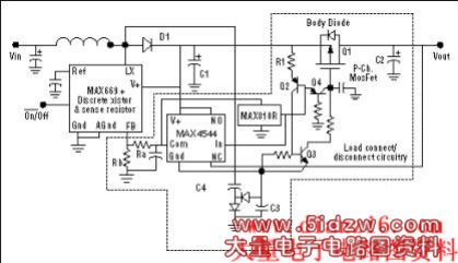
Figure 5. To achieve the load disconnect for low output voltages, this circuit ensures adequate drive to the MOSFET by generating a negative rail for the gate-drive IC (MAX810L).
Although Q1 turns on when the MAX810 output goes low, the MAX810's reset threshold cannot accurately sense the main output voltage with its ground terminal referred to the negative charge-pump output. Accordingly, the MAX810 ground terminal connects to ground and its output drives a level shifter comprised of Q2 and Q3, such that Q1's gate is pulled to the negative rail for turn-on.
The MAX668 features Idle Mode™ pulse frequency modulation (PFM) at light loads, which allows it to skip charging pulses when load current from the main supply is low. When pulses are skipped, Q2's emitter current (set by R1) discharges C3. This action can result in insufficient supply voltage to the MAX4544, even with the main output voltage in regulation. In turn, this effect can cause the on-resistance to skyrocket in the internal analog switch and the feedback voltage at the MAX668 to drop toward ground.
,A Smart Solid-State Fuse Cures
If the external load or the charging of C2 draws a heavy current at startup, such that a fast turn-on of Q1 could cause the MAX810 to issue a reset, an RC network can be added to slow the turn-on (Figure 3). A proper selection of these components can apply the load over multiple switching cycles of the MAX668, enabling its output voltage to remain above the reset threshold. Slowing the Q1 turn-on may be desirable, but slowing the turn-off may not be. Accordingly, the circuit includes a Schottky diode in parallel with the resistor to disable Q1 quickly in response to an excessive and unexpected load.
Figure 3. Adding three components in the MOSFET-gate circuit of Figure 2 provides the slow-connect/fast-disconnect necessary to accommodate heavy startup loads.
These circuits require a logic-level p-channel MOSFET such as Q1 to fully enhance the channel and obtain a low Rds-on. If Q1's on-resistance is high enough to cause a significant voltage drop (especially in low-output-voltage applications, or if the load is relatively far away), then it can be desirable to regulate the drain side of Q1. In doing this, you should minimize parasitics and observe good circuit-layout techniques. This remote regulation can be implemented with a SPDT, low-voltage analog switch in a SOT23 package (MAX4544), controlled by the MAX810's output state (Figure 4).
Figure 4. Further embellishments (to Figure 3) add remote-sense regulation and low-voltage detection to the boost converter with load disconnect.
The MAX4544 operates within data-sheet limits for supply voltages as low as 2.7V. With the input supply at 3.3V and about 0.3V across the Schottky diode, the MAX4544 (and MAX810) remains operational even when the boost converter is shut down. The MAX810 output is high during shutdown, connecting the MAX4544 COM node to NO (the Q1 source). When the boost converter turns on, resistors connected to the MAX4544 COM pin provide feedback to the MAX668. MAX4544 on-resistance is 60Ω maximum with a 5V supply, so the feedback-resistor values should be much larger than that to minimize output-voltage errors. On-resistance is only 120Ω at 3V; thus, the MAX4544 switch errors are minimal even for lower output voltages.
When the boost circuit is enabled and after the timeout period has elapsed, the MAX810 output goes low and connects the load by means of Q1. Simultaneously, the MAX810 output also causes the feedback resistors to switch over to the drain side of Q1, thus allowing output-voltage regulation at the load, which is remote to the main boost circuit.
This action also switches the MAX810 input to the drain side of Q1, where it can monitor overload conditions at the load. The foregoing arrangement is especially valuable if Q1's Rds-on causes a voltage drop greater than ~1% at the maximum load current. This can happen if Rds-on > 50mΩ at > 1A output on a 5V supply.
In response to a current overload, the MAX810 output goes high and quickly turns off Q1 through the Schottky diode. Simultaneously, it switches itself and the feedback resistors back to the source (input) side of Q1. The preceding configuration gives the boost output a chance to get back into regulation, after which the MAX810 reconnects the load. This cycle repeats until the overload is removed.
The MAX4544's break-before-make switching action is rather quick (10ns), so a small capacitor across the feedback resistors maintains the output voltage during the break period, to avoid disrupting the MAX668 feedback loop and to provide power to the MAX810. To prevent appreciable effects on the MAX668 transient response, this capacitor should be large enough to avoid significant discharge during the break period yet small enough to ensure a small time constant with the MAX4544 on-resistances.
The MAX4544's switch-control input has no Schmitt trigger, but it can tolerate slowly moving logic-level signals (these signals can, however, cause a 10-4A order of current to flow during the transition from the supply node to ground). The actual switch action is quick once the switching threshold is reached.
When using the MAX669 to boost low output voltages of 2.5V and below, a negative voltage may be required to fully enhance Q1. For example, an inexpensive, discrete charge pump attached to the LX node can generate -Vout + Vd (Figure 5). For a 2.7V output, it produces -2.0V with a standard pn-junction diode or -2.4V with a Schottky diode. This voltage is present whenever the boost converter is enabled, and it provides both a negative supply for the MAX4544 (which tolerates supply voltages to 12V) and biasing for Q1.
Figure 5. To achieve the load disconnect for low output voltages, this circuit ensures adequate drive to the MOSFET by generating a negative rail for the gate-drive IC (MAX810L).
Although Q1 turns on when the MAX810 output goes low, the MAX810's reset threshold cannot accurately sense the main output voltage with its ground terminal referred to the negative charge-pump output. Accordingly, the MAX810 ground terminal connects to ground and its output drives a level shifter comprised of Q2 and Q3, such that Q1's gate is pulled to the negative rail for turn-on.
The MAX668 features Idle Mode™ pulse frequency modulation (PFM) at light loads, which allows it to skip charging pulses when load current from the main supply is low. When pulses are skipped, Q2's emitter current (set by R1) discharges C3. This action can result in insufficient supply voltage to the MAX4544, even with the main output voltage in regulation. In turn, this effect can cause the on-resistance to skyrocket in the internal analog switch and the feedback voltage at the MAX668 to drop toward ground.
,A Smart Solid-State Fuse Cures